Solutions for etching printed circuit boards. Etching boards with hydrogen peroxide and citric acid. Applying a protective mask
How to etch a printed circuit board.
For those who are just starting to engage in amateur radio design, or simply do not know how to make a printed circuit board, in this article we will present several options for etching using chemical reagents.
We would like to note right away that most radio amateurs use ferric chloride for etching boards; we will consider this option, as well as several alternatives, but we will not dwell on etching using hydrochloric and nitric acids, and many other unsafe or confusing methods. Let's consider only those options that can actually be applied at home, and quickly. So, let's go in order.
Board etching option 1.
Ferric chloride.

Usually on the packaging the manufacturer writes in what ratio the ferric chloride solution is prepared. As a rule, this is 1: 3 (one to three), that is, 30...40 grams of ferric chloride crystals are dissolved in 100 grams of water. The etching time of the board depends on the concentration of the solution, as well as on the temperature of the solution; in a heated solution (up to 60 degrees) etching proceeds much faster. It is necessary to etch in a plastic or glass bath, and it is better to use a plastic spoon to prepare the solution.
On the Internet, we came across information on how to prepare a ferric chloride solution yourself. To do this, 15 grams of small iron filings are poured into 250 ml of 10% hydrochloric acid (a glass), and the solution is infused for several days until it turns brown. When it has settled, you can start etching.
The board is placed in the etching bath with the etching side down. To prevent the board from sinking to the very bottom, many radio amateurs glue it to Double-sided tape a piece of foam plastic to the top side of the board. If you need to etch a double-sided board, place it vertically in a tray or jar. This way, the dissolved copper will settle more easily to the bottom of the container and the etching process will be faster.
Do not let the ferric chloride solution come into contact with your clothing; it will be damaged and the stains will most likely not be removed.
Board etching option 2.
Copper sulfate + table salt.

As you probably know, copper sulfate It is a bluish crystal, can be purchased at hardware stores or gardening stores, in general, there is no shortage. Salt - regular coarse salt from the grocery store.
In addition to salt and vitriol, we will also need some small iron object (an iron plate, a nail, or something else), which we will place in the solution next to the board during etching. We will not go into the intricacies of chemical processes, we will only note that this process occurs with the formation of many complex salts, and an iron object placed in a solution during etching enters into this reaction and is consumed in the process. The solution is prepared from one part copper sulfate and two parts table salt.

That is, put four heaped tablespoons of copper sulfate on two heaped tablespoons of copper sulfate, pour in one and a half glasses of hot water (70 degrees), stir until the crystals are completely dissolved, and the etching solution is ready. Do not make a mixture of vitriol and salt crystals in advance; first dissolve one component and then the other.
Etching time is approximately 40 minutes.
Even if you do not use an iron object when etching, the board will also be etched.
If bluish spots remain on the board after etching, they can be easily removed with vinegar.
Board etching option 3.
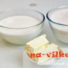
Hydrogen peroxide + citric acid + table salt.

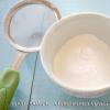
The recipe for this solution for etching boards is simple: in 100 grams of ordinary pharmacy 3% hydrogen peroxide, dissolve approximately 30 grams of citric acid and 5 grams of table salt. Stir until all bulk ingredients are completely dissolved, and the solution is ready for use.
We draw your attention to the fact that there is no need to pour water into the solution. And lastly, this solution is not stored or reused. The amount prepared in this way is enough to etch about 100 square meters. cm copper foil with a thickness of 35 microns. For further etching, the solution is prepared again.
We hope that from these three options you will surely choose the one that suits you best, based on what you have on your this moment there is time at hand.
After the printed circuit board design is transferred to the foil-coated PCB using , it is necessary to etch the printed circuit board. Several pickling recipes printed circuit boards are described under the cut.
1. Method one - ferric chloride.

Add ferric chloride to water in a ratio of 1:3. To stir thoroughly.
The etching time depends on the temperature of the solution, the thickness of the copper and the “freshness” of the solution.
On average from 10 minutes to an hour. When applying tracks with laser printer toner, do not heat it above 45°C.
It is recommended to rock the board in the solution.
2. Method two - copper sulfate plus table salt.

Preparation of solution - 200 ml. warm water, two tablespoons of table salt and a tablespoon of copper sulfate. The etching process can be quite lengthy.

For the etching process to proceed normally, it is recommended to use a significant excess of salt, heat the solution and rock the board in the solution.
3. Etching the printed circuit board in hydrogen peroxide plus citric acid.
A fairly quick method of etching a printed circuit board with room temperature plus the availability of components.

Solution composition:
In 100 ml. Dissolve 3% hydrogen peroxide with 30 g of citric acid and 5 g of table salt.

Salt can be given in excess.
The solution should not be diluted. The more peroxide, the more intense the process will be.
But we must take into account that the solution is disposable and cannot be stored.
Printed circuit board– this is a dielectric base, on the surface and in the volume of which conductive paths are applied in accordance with the electrical circuit. The printed circuit board is designed for mechanical fastening and electrical connection between each other by soldering the leads of electronic and electrical products installed on it.
The operations of cutting out a workpiece from fiberglass, drilling holes and etching a printed circuit board to obtain current-carrying tracks, regardless of the method of applying the pattern to the printed circuit board, are performed using the same technology.
Manual application technology
PCB tracks
Preparing the template
The paper on which the PCB layout is drawn is usually thin and for more accurate drilling of holes, especially when using manual homemade drill so that the drill does not lead to the side, it is necessary to make it more dense. To do this, you need to glue the printed circuit board design onto thicker paper or thin thick cardboard using any glue, such as PVA or Moment.

Cutting the workpiece
A blank of foil fiberglass laminate of a suitable size is selected, the printed circuit board template is applied to the blank and outlined around the perimeter with a marker, a soft pencil or marking with a sharp object.

Next, the fiberglass laminate is cut along the marked lines using metal scissors or sawed out with a hacksaw. Scissors cut faster and there is no dust. But we must take into account that when cutting with scissors, fiberglass is strongly bent, which somewhat worsens the adhesion strength of copper foil and if the elements need to be re-soldered, the tracks may peel off. Therefore, if the board is large and has very thin traces, then it is better to cut it using a hacksaw.

The template of the printed circuit board pattern is glued to the cut-out workpiece using Moment glue, four drops of which are applied to the corners of the workpiece.

Since the glue sets in just a few minutes, you can immediately begin drilling holes for radio components.
Drilling holes
It is best to drill holes using a special mini drilling machine with a carbide drill with a diameter of 0.7-0.8 mm. If a mini drilling machine is not available, then you can drill holes with a low-power drill using a simple drill. But when working with a universal hand drill, the number of broken drills will depend on the hardness of your hand. You definitely won’t be able to get by with just one drill.

If you cannot clamp the drill, you can wrap its shank with several layers of paper or one layer of sandpaper. You can wrap a thin metal wire tightly around the shank, turn to turn.

After finishing drilling, check whether all holes are drilled. This can be clearly seen if you look at the printed circuit board up to the light. As you can see, there are no missing holes.
Applying a topographic drawing
In order to protect the places of foil on fiberglass laminate that will be conductive paths from destruction during etching, they must be covered with a mask that is resistant to dissolution in an aqueous solution. For the convenience of drawing paths, it is better to pre-mark them using a soft pencil or marker.
Before applying the markings, it is necessary to remove traces of the glue that was used to glue the printed circuit board template. Since the glue has not hardened much, it can be easily removed by rolling it with your finger. The surface of the foil must also be degreased using a rag using any means, such as acetone or white alcohol (the so-called purified gasoline), or any dishwashing detergent, for example Ferry.

After marking the tracks of the printed circuit board, you can begin to apply their design. Any waterproof enamel is well suited for drawing paths, for example alkyd enamel of the PF series, diluted to a suitable consistency with a white alcohol solvent. You can draw paths different instruments– a glass or metal drawing pen, a medical needle and even a toothpick. In this article I will tell you how to draw circuit board traces using a drawing pen and ballerina, which are designed for drawing on paper with ink.

Previously, there were no computers and all drawings were drawn with simple pencils on whatman paper and then transferred in ink to tracing paper, from which copies were made using copiers.
Drawing begins with contact pads, which are drawn with a ballerina. To do this, you need to adjust the gap of the sliding jaws of the ballerina drawing board to the required line width and to set the diameter of the circle, perform the adjustment with the second screw, moving the drawing blade away from the axis of rotation.
Next, the ballerina's drawing board is filled with paint to a length of 5-10 mm using a brush. For applying a protective layer to a printed circuit board, PF or GF paint is best suited, since it dries slowly and allows you to work quietly. NTs brand paint can also be used, but it is difficult to work with because it dries quickly. The paint should adhere well and not spread. Before painting, the paint must be diluted to a liquid consistency, adding a suitable solvent to it little by little with vigorous stirring and trying to paint on scraps of fiberglass. To work with paint, it is most convenient to pour it into a bottle of manicure varnish, in the twist of which there is a solvent-resistant brush installed.
After adjusting the ballerina's drawing board and obtaining the required line parameters, you can begin to apply the contact pads. To do this, the sharp part of the axis is inserted into the hole and the base of the ballerina is rotated in a circle.

With the correct setting of the drawing pen and the desired consistency of paint around the holes on the printed circuit board, perfectly round circles are obtained. When a ballerina begins to paint poorly, the remaining dried paint is removed from the gap of the drawing board with a cloth and the drawing board is filled with fresh paint. To draw all the holes on this printed circuit board with circles it took only two refills of the drawing pen and no more than two minutes of time.
Once the round pads on the board are drawn, you can start drawing the conductive paths using a hand drawing pen. Preparing and adjusting a manual drawing board is no different from preparing a ballerina.
The only thing additionally needed is a flat ruler, with pieces of rubber 2.5-3 mm thick glued to one of its sides along the edges, so that the ruler does not slip during operation and the fiberglass, without touching the ruler, can freely pass under it. A wooden triangle is best suited as a ruler; it is stable and at the same time can serve as a hand support when drawing a printed circuit board.

To prevent the printed circuit board from slipping when drawing tracks, it is advisable to place it on a sheet of sandpaper, which consists of two sandpaper sheets sealed together with the paper sides.

If they come into contact when drawing paths and circles, then you should not take any measures. You need to let the paint on the printed circuit board dry until it does not stain when touched, and use the tip of a knife to remove the excess part of the design. In order for the paint to dry faster, the board should be placed in a warm place, for example in winter time to the heating battery. IN summer time years - under the rays of the sun.

When the design on the printed circuit board is completely applied and all defects are corrected, you can proceed to etching it.
Printed circuit board design technology
using a laser printer
When printing on a laser printer, the image formed by the toner is transferred, due to electrostatics, from the photo drum on which the laser beam drew the image, onto paper. The toner is held onto the paper, preserving the image, only due to electrostatics. To fix the toner, the paper is rolled between rollers, one of which is a thermal oven heated to a temperature of 180-220°C. The toner melts and penetrates the paper texture. Once cooled, the toner hardens and adheres firmly to the paper. If the paper is heated again to 180-220°C, the toner will again become liquid. This property of toner is used to transfer images of current-carrying tracks onto a printed circuit board at home.
After the file with the printed circuit board design is ready, you need to print it using a laser printer onto paper. Please note that the image of the printed circuit board drawing for this technology must be viewed from the side where the parts are installed! An inkjet printer is not suitable for these purposes, as it works on a different principle.
Preparing a paper template for transferring the design to the printed circuit board
If you print a printed circuit board design on ordinary paper for office equipment, then due to its porous structure, the toner will penetrate deeply into the body of the paper and when the toner is transferred to the printed circuit board, most of it will remain in the paper. In addition, there will be difficulties in removing paper from the printed circuit board. You will have to soak it in water for a long time. Therefore, to prepare a photomask, you need paper that does not have a porous structure, for example photo paper, a substrate from self-adhesive films and labels, tracing paper, pages from glossy magazines.
I use old stock tracing paper as the paper for printing the PCB design. Tracing paper is very thin and it is impossible to print a template directly on it; it gets jammed in the printer. To solve this problem, before printing, you need to apply a drop of any glue to a piece of tracing paper of the required size in the corners and glue it to a sheet of A4 office paper.

This technique allows you to print a printed circuit board design even on the thinnest paper or film. In order for the toner thickness of the drawing to be maximum, before printing, you need to configure the “Printer Properties” by turning off the economical printing mode, and if this function is not available, then select the coarsest type of paper, for example cardboard or something similar. It’s entirely possible that you won’t get a good print the first time, and you’ll have to experiment a little to find the best print mode for your laser printer. In the resulting print of the design, the tracks and contact pads of the printed circuit board must be dense without gaps or smudging, since retouching at this technological stage is useless.

All that remains is to cut the tracing paper along the contour and the template for making the printed circuit board will be ready and you can proceed to the next step, transferring the image onto fiberglass laminate.
Transferring a design from paper to fiberglass
Transferring the printed circuit board design is the most critical step. The essence of the technology is simple: paper, with the side of the printed pattern of the tracks of the printed circuit board, is applied to the copper foil of fiberglass and pressed with great force. Next, this sandwich is heated to a temperature of 180-220°C and then cooled to room temperature. The paper is torn off, and the design remains on the printed circuit board.
Some craftsmen suggest transferring a design from paper to a printed circuit board using an electric iron. I tried this method, but the result was unstable. It is difficult to simultaneously ensure that the toner is heated to the required temperature and that the paper is pressed evenly onto the entire surface of the printed circuit board when the toner hardens. As a result, the pattern is not completely transferred and gaps remain in the pattern of the printed circuit board tracks. Perhaps the iron was not heating up enough, although the regulator was set to maximum iron heating. I didn’t want to open the iron and reconfigure the thermostat. Therefore, I used another technology, less labor-intensive and providing one hundred percent results.
On a piece of foil fiberglass laminate cut to the size of the printed circuit board and degreased with acetone, I glued tracing paper with a pattern printed on it in the corners. On top of the tracing paper I placed, for more even pressure, heels of sheets of office paper. The resulting package was placed on a sheet of plywood and covered on top with a sheet of the same size. This entire sandwich was clamped with maximum force in clamps.

All that remains is to heat the prepared sandwich to a temperature of 200°C and cool. An electric oven with a temperature controller is ideal for heating. It is enough to place the created structure in the closet and wait for the set set temperature and after half an hour, remove the board to cool.

If you don’t have an electric oven, you can use a gas oven by adjusting the temperature using the gas supply knob using the built-in thermometer. If there is no thermometer or it is faulty, then women can help; the position of the control knob at which pies are baked is suitable.

Since the ends of the plywood were warped, I clamped them with additional clamps just in case. To avoid this phenomenon, it is better to clamp the printed circuit board between metal sheets 5-6 mm thick. You can drill holes in their corners and clamp printed circuit boards, tighten the plates using screws and nuts. M10 will be enough.
After half an hour, the structure has cooled enough for the toner to harden, and the board can be removed. At the first glance at the removed printed circuit board, it becomes clear that the toner transferred from tracing paper to the board perfectly. The tracing paper fit tightly and evenly along the lines of the printed tracks, rings of contact pads and marking letters.

The tracing paper easily came off from almost all the traces of the printed circuit board; the remaining tracing paper was removed with a damp cloth. But still, there were gaps in several places on the printed tracks. This can happen as a result of uneven printing from the printer or remaining dirt or corrosion on the fiberglass foil. Gaps can be painted over with any waterproof paint, manicure polish, or retouched with a marker.

To check the suitability of a marker for retouching a printed circuit board, you need to draw lines on paper with it and moisten the paper with water. If the lines do not blur, then the retouching marker is suitable.

It is best to etch a printed circuit board at home in a solution of ferric chloride or hydrogen peroxide with citric acid. After etching, toner can be easily removed from the print tracks with a swab soaked in acetone.
Then holes are drilled, conductive paths and contact pads are tinned, and radioelements are sealed.

This is the appearance of the printed circuit board with radio components installed on it. The result was a power supply and switching unit for electronic system, complementing an ordinary toilet with a bidet function.
PCB etching
To remove copper foil from unprotected areas of foiled fiberglass laminate when making printed circuit boards at home, radio amateurs usually use chemical method. The printed circuit board is placed in an etching solution and due to chemical reaction copper, unprotected by the mask, dissolves.
Recipes for pickling solutions
Depending on the availability of components, radio amateurs use one of the solutions given in the table below. Etching solutions are arranged in order of popularity of their use by radio amateurs at home.
| Name of solution | Compound | Quantity | Cooking technology | Advantages | Flaws |
|---|---|---|---|---|---|
| Hydrogen peroxide plus citric acid | Hydrogen peroxide (H 2 O 2) | 100 ml | Dissolve citric acid and table salt in a 3% solution of hydrogen peroxide. | Availability of components, high etching speed, safety | Not stored |
| Citric acid (C 6 H 8 O 7) | 30 g | ||||
| Table salt (NaCl) | 5 g | ||||
| Aqueous solution of ferric chloride | Water (H2O) | 300 ml | IN warm water dissolve ferric chloride | Sufficient etching speed, reusable | Low availability of ferric chloride |
| Ferric chloride (FeCl 3) | 100 g | Hydrogen peroxide plus hydrochloric acid | Hydrogen peroxide (H 2 O 2) | 200 ml | Pour 10% hydrochloric acid into a 3% hydrogen peroxide solution. | High etching rate, reusable | Great care required |
| Hydrochloric acid (HCl) | 200 ml | ||||
| Aqueous solution of copper sulfate | Water (H2O) | 500 ml | IN hot water(50-80°C) dissolve table salt, and then copper sulfate | Component Availability | The toxicity of copper sulfate and slow etching, up to 4 hours |
| Copper sulfate (CuSO 4) | 50 g | ||||
| Table salt (NaCl) | 100 g | ||||
Etch printed circuit boards in metal utensils not allowed. To do this, you need to use a container made of glass, ceramic or plastic. The used etching solution may be disposed of in the sewer system.
Etching solution of hydrogen peroxide and citric acid
A solution based on hydrogen peroxide with citric acid dissolved in it is the safest, most affordable and fastest working. Of all the solutions listed, this is the best by all criteria.

Hydrogen peroxide can be purchased at any pharmacy. Sold in the form of a liquid 3% solution or tablets called hydroperite. To obtain a liquid 3% solution of hydrogen peroxide from hydroperite, you need to dissolve 6 tablets weighing 1.5 grams in 100 ml of water.
Citric acid in the form of crystals is sold in any grocery store, packaged in bags weighing 30 or 50 grams. Table salt can be found in any home. 100 ml of etching solution is enough to remove 35 micron thick copper foil from a printed circuit board with an area of 100 cm 2. The used solution is not stored and cannot be reused. By the way, citric acid can be replaced with acetic acid, but because of its pungent odor, you will have to etch the printed circuit board outdoors.
Ferric chloride pickling solution
The second most popular etching solution is an aqueous solution of ferric chloride. Previously, it was the most popular, since ferric chloride was easy to obtain at any industrial enterprise.

The etching solution is not demanding on temperature; it etches quickly enough, but the etching rate decreases as the ferric chloride in the solution is consumed.

Ferric chloride is very hygroscopic and therefore quickly absorbs water from the air. As a result, a yellow liquid appears at the bottom of the jar. This does not affect the quality of the component and such ferric chloride is suitable for preparing an etching solution.
If the used ferric chloride solution is stored in an airtight container, it can be reused many times. Subject to regeneration, just pour iron nails into the solution (they will immediately be covered with a loose layer of copper). If it gets on any surface, it leaves a difficult-to-remove yellow spots. Currently, ferric chloride solution is used less frequently for the manufacture of printed circuit boards due to its high cost.
Etching solution based on hydrogen peroxide and hydrochloric acid
Excellent etching solution, provides high etching speed. Hydrochloric acid, with vigorous stirring, is poured into a 3% aqueous solution of hydrogen peroxide in a thin stream. It is unacceptable to pour hydrogen peroxide into acid! But due to the presence of hydrochloric acid in the etching solution, great care must be taken when etching the board, since the solution corrodes the skin of the hands and spoils everything it comes into contact with. For this reason, it is not recommended to use an etching solution with hydrochloric acid at home.
Etching solution based on copper sulfate
The method of manufacturing printed circuit boards using copper sulfate is usually used if it is impossible to produce an etching solution based on other components due to their inaccessibility. Copper sulfate is a pesticide and is widely used for pest control in agriculture. In addition, the etching time of the printed circuit board is up to 4 hours, while it is necessary to maintain the solution temperature at 50-80°C and ensure a constant change of the solution at the surface being etched.
PCB etching technology
For etching the board in any of the above etching solutions, glass, ceramic or plastic dishes, for example from dairy products, are suitable. If you don’t have a suitable size container at hand, you can take any box of thick paper or cardboard of a suitable size and line its inside plastic film. An etching solution is poured into the container and a printed circuit board is carefully placed on its surface, pattern down. Due to the forces of surface tension of the liquid and its light weight, the board will float.

For convenience, you can glue a plastic bottle cap to the center of the board with instant glue. The cork will simultaneously serve as a handle and a float. But there is a danger that air bubbles will form on the board and the copper will not be etched in these places.

To ensure uniform etching of copper, you can place the printed circuit board on the bottom of the container with the pattern facing up and periodically shake the tray with your hand. After some time, depending on the etching solution, areas without copper will begin to appear, and then the copper will completely dissolve on the entire surface of the printed circuit board.

After the copper is completely dissolved in the etching solution, the printed circuit board is removed from the bath and thoroughly washed under running water. Toner is removed from the tracks with a rag soaked in acetone, and paint is easily removed with a rag soaked in a solvent that was added to the paint to obtain the desired consistency.
Preparing the printed circuit board for installation of radio components
The next step is to prepare the printed circuit board for the installation of radio elements. After removing the paint from the board, the tracks need to be processed in a circular motion with fine sandpaper. There is no need to get carried away, because the copper tracks are thin and can be easily ground off. Just a few passes with abrasive with light pressure are enough.

Next, the current-carrying paths and contact pads of the printed circuit board are coated with alcohol-rosin flux and tinned soft solder electric soldering iron. To prevent the holes on the printed circuit board from being covered with solder, you need to take a little bit of it onto the soldering iron tip.

After completing the manufacture of the printed circuit board, all that remains is to insert the radio components into the designated positions and solder their leads to the pads. Before soldering, the legs of the parts must be moistened with alcohol-rosin flux. If the legs of the radio components are long, then before soldering they need to be cut with side cutters to a protrusion length above the surface of the printed circuit board of 1-1.5 mm. After completing the installation of parts, you need to remove any remaining rosin using any solvent - alcohol, white alcohol or acetone. They all successfully dissolve rosin.

It took no more than five hours to implement this simple capacitive relay circuit from laying out the tracks for manufacturing a printed circuit board to creating a working sample, much less than it took to type up this page.
It is difficult to remove ferric chloride from a sink or a kitchen towel. It's hard to explain the acid hole in my pants to my wife. I'm in Lately switched to the cheapest and cleanest method of etching printed circuit boards. Thanks to the unknown chemist who first described this method on the Internet. Unfortunately, I don’t remember where or who he is.
Later, I saw similar recipes many times on different sites on the Internet, and decided to add this cheat sheet to Datagor, so that it is always at hand and in the appropriate section. This method of etching boards is great for both beginning radio amateurs and elders.
To chemicalize the etching solution we need safe and affordable potions
☂️ Please note that there is no water in the recipe!
⚖️ This amount of solution is enough to etch ≈100 cm²
copper foil standard thickness 35 microns.
How to use the recipe?
All this must be mixed before use in glass or plastic containers. The amount of ingredients can be changed proportionally, and More citric acid is possible.Etching time approx. 20 minutes at room temperature, depends on the area of the board. Increasing the temperature does not lead to a significant increase in activity, so I believe that heating is not necessary.
It is important to stir the etching solution to access fresh solution and washing off reaction products.
Solution according to this recipe does not corrode hands and clothes and does not stain the sink. Initially, the solution is transparent, but as it is used, it acquires a “sea wave”, greenish-bluish color.

Photo in progress, sent to Datagor Beso(Minsk):
“Indeed, it poisons quickly, poisons cleanly, and, what is important,
poisons cheaper than ferric chloride"
LUT is suitable for correcting deficiencies permanent marker, paint marker or nail polish.
The solution is not stored, always it is better to poison in a freshly prepared mixture.

My version of pickling in a bucket of some kind of food.
The solution is used very economically.
The Internet also offers an option to replace citric acid with 70% acetic acid. I believe that this can only be done as a last resort, because we end up with a stink and working in a more dangerous environment.
Tahiti!.. Tahiti!..
We have not been to any Tahiti!
They feed us well here too!
© Cartoon cat
Introduction with digression
How were boards made in the past in domestic and laboratory conditions? There were several ways, for example:
- future conductors drew drawings;
- engraved and cut with cutters;
- they glued it with adhesive tape or tape, then cut out the design with a scalpel;
- They made simple stencils and then applied the design using an airbrush.
The missing elements were completed with drawing pens and retouched with a scalpel.
It was a long and labor-intensive process, requiring the “drawer” to have remarkable artistic abilities and accuracy. The thickness of the lines hardly fit into 0.8 mm, there was no repetition accuracy, each board had to be drawn separately, which greatly limited the production of even a very small batch printed circuit boards(further PP).
What do we have today?
Progress does not stand still. The times when radio amateurs painted PP with stone axes on mammoth skins have sunk into oblivion. The appearance on the market of publicly available chemistry for photolithography opens up completely different prospects for us to produce PCB without metallization of holes at home.
Let's take a quick look at the chemistry used today to produce PP.
Photoresist
You can use liquid or film. We will not consider film in this article due to its scarcity, difficulties in rolling onto PCBs and the lower quality of the resulting printed circuit boards.
After analyzing market offers, I settled on POSITIV 20 as the optimal photoresist for home PCB production.
Purpose:
POSITIV 20 photosensitive varnish. Used in small-scale production of printed circuit boards, copper engravings, and when carrying out work related to transferring images to various materials.
Properties:
High exposure characteristics provide good contrast of transferred images.
Application:
It is used in areas related to the transfer of images onto glass, plastics, metals, etc. in small-scale production. Directions for use are indicated on the bottle.
Characteristics:
Color: blue
Density: at 20°C 0.87 g/cm 3
Drying time: at 70°C 15 min.
Consumption: 15 l/m2
Maximum photosensitivity: 310-440 nm
The instructions for the photoresist say that it can be stored at room temperature and is not subject to aging. I strongly disagree! It should be stored in a cool place, for example, on the bottom shelf of the refrigerator, where the temperature is usually maintained at +2+6°C. But under no circumstances allow negative temperatures!
If you use photoresists that are sold by the glass and do not have lightproof packaging, you need to take care of protection from light. It should be stored in complete darkness and at a temperature of +2+6°C.
Enlightener
Likewise, I consider TRANSPARENT 21, which I constantly use, to be the most suitable educational tool.
Purpose:
Allows direct transfer of images onto surfaces coated with photosensitive emulsion POSITIV 20 or other photoresist.
Properties:
Gives transparency to paper. Provides transmission of ultraviolet rays.
Application:
For quickly transferring the outlines of drawings and diagrams onto a substrate. Allows you to significantly simplify the reproduction process and reduce time s e costs.
Characteristics:
Color: transparent
Density: at 20°C 0.79 g/cm 3
Drying time: at 20°C 30 min.
Note:
Instead of regular paper with transparency, you can use transparent film for inkjet or laser printers, depending on what we will print the photomask on.
Photoresist developer
There are many different solutions for developing photoresist.
It is advised to develop using a solution " liquid glass" His chemical composition: Na 2 SiO 3 * 5H 2 O. This substance has a huge number of advantages. The most important thing is that it is very difficult to overexpose the PP in it; you can leave the PP for a non-fixed exact time. The solution almost does not change its properties with temperature changes (there is no risk of disintegration with increasing temperature), it also has a very long term storage its concentration remains constant for at least a couple of years. The absence of the problem of overexposure in the solution will allow increasing its concentration to reduce the time of development of PP. It is recommended to mix 1 part concentrate with 180 parts water (just over 1.7 g of silicate in 200 ml of water), but it is possible to make a more concentrated mixture so that the image develops in about 5 seconds without the risk of surface damage due to overexposure. If it is impossible to purchase sodium silicate, use sodium carbonate (Na 2 CO 3) or potassium carbonate (K 2 CO 3).
I haven’t tried either the first or the second, so I’ll tell you what I’ve been using without any problems for several years now. I use a water solution of caustic soda. For 1 liter cold water 7 grams of caustic soda. If there is no NaOH, I use a KOH solution, doubling the concentration of alkali in the solution. Development time 30-60 seconds with correct exposure. If after 2 minutes the pattern does not appear (or appears weakly), and the photoresist begins to wash off from the workpiece, this means that the exposure time was chosen incorrectly: you need to increase it. If, on the contrary, it quickly appears, but both exposed and unexposed areas are washed away; either the concentration of the solution is too high, or the quality of the photomask is low (ultraviolet light passes freely through the “black”): you need to increase the print density of the template.
Copper etching solutions
Excess copper is removed from printed circuit boards using various etchants. Among people doing this at home, ammonium persulfate, hydrogen peroxide + hydrochloric acid, copper sulfate solution + table salt are often common.
I always poison with ferric chloride in a glass container. When working with the solution, you need to be careful and attentive: if it gets on clothes and objects, it leaves rusty stains that are difficult to remove. weak solution citric (lemon juice) or oxalic acid.
We heat a concentrated solution of ferric chloride to 50-60°C, immerse the workpiece in it, and carefully and effortlessly move a glass rod with a cotton swab at the end over areas where copper is etched less easily, this achieves a more even etching over the entire area of the PP. If you do not force the speed to equalize, the required etching duration increases, and this eventually leads to the fact that in areas where copper has already been etched, etching of the tracks begins. As a result, we don’t get what we wanted at all. It is highly desirable to ensure continuous stirring of the etching solution.
Chemicals for removing photoresist
What is the easiest way to wash off unnecessary photoresist after etching? After repeated trial and error, I settled on ordinary acetone. When it is not there, I wash it off with any solvent for nitro paints.
So, let's make a printed circuit board
Where does a high quality PCB start? Right:
Create a high-quality photo template
To make it, you can use almost any modern laser or inkjet printer. Considering that we are using positive photoresist in this article, the printer should draw black where copper should remain on the PCB. Where there should be no copper the printer should not draw anything. Very important point when printing a photomask: you need to set the maximum dye flow (in the printer driver settings). The blacker the painted areas, the greater the chances of getting a great result. No color is needed, a black cartridge is enough. From the program (we will not consider programs: everyone is free to choose for themselves - from PCAD to Paintbrush) in which the photo template was drawn, we print it on a regular sheet of paper. The higher the printing resolution and the higher quality the paper, the higher the quality of the photomask. I recommend no lower than 600 dpi; the paper should not be very thick. When printing, we take into account that with the side of the sheet on which the paint is applied, the template will be placed on the PP blank. If done differently, the edges of the PP conductors will be blurred and indistinct. Let the paint dry if it was an inkjet printer. Next, we impregnate the paper with TRANSPARENT 21, let it dry and the photo template is ready.
Instead of paper and enlightenment, it is possible and even very desirable to use transparent film for laser (when printing on a laser printer) or inkjet (for inkjet printing) printers. Please note that these films have unequal sides: only one working side. If you use laser printing, I highly recommend dry running a sheet of film before printing - simply run the sheet through the printer, simulating printing, but not printing anything. Why is this necessary? When printing, the fuser (oven) will heat the sheet, which will inevitably lead to its deformation. As a consequence, there is an error in the geometry of the output PCB. When producing double-sided PCBs, this is fraught with a mismatch of layers with all the consequences And with the help of a “dry” run, we will warm up the sheet, it will be deformed and will be ready for printing the template. When printing, the sheet will pass through the oven a second time, but the deformation will be much less significant checked several times.
If the PP is simple, you can draw it manually in a very convenient program with a Russified interface Sprint Layout 3.0R (~650 KB).

On preparatory stage draw not too bulky electrical circuits very convenient in the also Russified program sPlan 4.0 (~450 KB).

This is what the finished photo templates look like, printed on an Epson Stylus Color 740 printer:


We print only in black, with maximum dye addition. Material transparent film for inkjet printers.
Preparing the PP surface for applying photoresist
For the production of PP they are used sheet materials with applied copper foil. The most common options are with copper thicknesses of 18 and 35 microns. Most often, for the production of PP at home, sheet textolite (fabric pressed with glue in several layers), fiberglass (the same, but epoxy compounds are used as glue) and getinax (pressed paper with glue) are used. Less commonly, sittal and polycor (high-frequency ceramics are used extremely rarely at home), fluoroplastic (organic plastic). The latter is also used for the manufacture of high-frequency devices and, having very good electrical characteristics, can be used anywhere and everywhere, but its use is limited by its high price.
First of all, you need to make sure that the workpiece does not have deep scratches, scuffs and corroded areas. Next, it is advisable to polish the copper to a mirror. We polish without being particularly zealous, otherwise we will erase the already thin layer of copper (35 microns) or, in any case, we will achieve different thicknesses of copper on the surface of the workpiece. And this, in turn, will lead to different etching rates: it will be etched faster where it is thinner. And a thinner conductor on the board is not always good. Especially if it is long and a decent current will flow through it. If the copper on the workpiece is of high quality, without sins, then it is enough to degrease the surface.
Applying photoresist to the surface of the workpiece
We place the board on a horizontal or slightly inclined surface and apply the composition from an aerosol package from a distance of about 20 cm. We remember that the most important enemy in this case is dust. Every particle of dust on the surface of the workpiece is a source of problems. To create a uniform coating, spray the aerosol in a continuous zigzag motion, starting from the upper left corner. Do not use the aerosol in excess quantities, as this will cause unwanted smudges and lead to the formation of a non-uniform coating thickness, requiring a longer exposure time. In summer at high temperatures environment Re-treatment may be necessary, or the aerosol may need to be sprayed from a shorter distance to reduce evaporation losses. When spraying, do not tilt the can too much; this leads to increased consumption of propellant gas and, as a result, the aerosol can stops working, although there is still photoresist in it. If you are getting unsatisfactory results when spray coating photoresist, use spin coating. In this case, photoresist is applied to a board mounted on a rotating table with a 300-1000 rpm drive. After finishing coating, the board should not be exposed to strong light. Based on the color of the coating, you can approximately determine the thickness of the applied layer:
- light gray blue 1-3 microns;
- dark gray blue 3-6 microns;
- blue 6-8 microns;
- dark blue more than 8 microns.
On copper, the coating color may have a greenish tint.
The thinner the coating on the workpiece, the better the result.
I always spin coat the photoresist. My centrifuge has a rotation speed of 500-600 rpm. Fastening should be simple, clamping is done only at the ends of the workpiece. We fix the workpiece, start the centrifuge, spray it on the center of the workpiece and observe how the photoresist the thinnest layer spreads over the surface. Centrifugal forces will throw off excess photoresist from the future PCB, so I highly recommend providing a protective wall so as not to turn the workplace into a pigsty. I use an ordinary saucepan with a hole in the bottom in the center. The axis of the electric motor passes through this hole, on which the mounting platform is installed in the form of a cross of two aluminum slats, along which the workpiece clamping ears “run”. The ears are made of aluminum angles, clamped to the rail with a wing nut. Why aluminum? Low specific gravity and, as a result, less runout when the center of mass of rotation deviates from the center of rotation of the centrifuge axis. The more accurately the workpiece is centered, the less beating will occur due to the eccentricity of the mass and the less effort will be required to rigidly attach the centrifuge to the base.
Photoresist is applied. Let it dry for 15-20 minutes, turn the workpiece over, apply a layer on the other side. Give another 15-20 minutes to dry. Do not forget that direct sunlight and fingers on the working sides of the workpiece are unacceptable.
Tanning photoresist on the surface of the workpiece
Place the workpiece in the oven, gradually bring the temperature to 60-70°C. Maintain at this temperature for 20-40 minutes. It is important that nothing touches the surfaces of the workpiece; only touching the ends is permissible.
Aligning the top and bottom photomasks on the workpiece surfaces
Each of the photo masks (top and bottom) should have marks along which 2 holes need to be made on the workpiece to align the layers. The farther the marks are from each other, the higher the alignment accuracy. I usually place them diagonally on the templates. Using a drilling machine, using these marks on the workpiece, we drill two holes strictly at 90° (the thinner the holes, the more accurate the alignment; I use a 0.3 mm drill) and align the templates along them, not forgetting that the template must be applied to the photoresist the side on which the print was made. We press the templates to the workpiece with thin glasses. It is preferable to use quartz glass as it transmits ultraviolet radiation better. Plexiglas (plexiglass) gives even better results, but it has the unpleasant property of scratching, which will inevitably affect the quality of the PP. For small PCB sizes, you can use a transparent cover from a CD package. In the absence of such glass, you can use ordinary window glass, increasing the exposure time. It is important that the glass is smooth, ensuring an even fit of the photomasks to the workpiece, otherwise it will be impossible to obtain high-quality edges of the tracks on the finished PCB.

A blank with a photomask under plexiglass. We use a CD box.
Exposure (light exposure)
The time required for exposure depends on the thickness of the photoresist layer and the intensity of the light source. Photoresist varnish POSITIV 20 is sensitive to ultraviolet rays, the maximum sensitivity occurs in the area with a wavelength of 360-410 nm.
It is best to expose under lamps whose radiation range is in the ultraviolet region of the spectrum, but if you do not have such a lamp, you can also use ordinary powerful incandescent lamps, increasing the exposure time. Do not start illumination until the lighting from the source has stabilized; it is necessary for the lamp to warm up for 2-3 minutes. The exposure time depends on the thickness of the coating and is usually 60-120 seconds when the light source is located at a distance of 25-30 cm. The glass plates used can absorb up to 65% of ultraviolet radiation, so in such cases it is necessary to increase the exposure time. top scores achieved using transparent plexiglass plates. When using photoresist with a long shelf life, the exposure time may need to be doubled remember: Photoresists are subject to aging!
Examples of using various sources Sveta:


UV lamps
We expose each side in turn, after exposure we let the workpiece stand for 20-30 minutes in a dark place.
Development of the exposed workpiece
We develop it in a solution of NaOH (caustic soda) see the beginning of the article for more details at a solution temperature of 20-25°C. If there is no manifestation within 2 minutes small O exposure time. If it appears well, but is washed off and useful areas you were too clever with the solution (the concentration is too high) or the exposure time for a given radiation source is too long or the photomask is of poor quality the insufficiently saturated printed black color allows ultraviolet light to illuminate the workpiece.
When developing, I always very carefully, effortlessly “roll” a cotton swab on a glass rod over the places where the exposed photoresist should wash off; this speeds up the process.
Washing the workpiece from alkali and residues of exfoliated exposed photoresist
I do it under water tap ordinary tap water.
Re-tanning photoresist
We place the workpiece in the oven, gradually raise the temperature and hold it at a temperature of 60-100°C for 60-120 minutes; the pattern becomes strong and hard.
Checking the development quality
Briefly (for 5-15 seconds) immerse the workpiece in a ferric chloride solution heated to a temperature of 50-60°C. Quickly rinse running water. In places where there is no photoresist, intensive etching of the copper begins. If photoresist accidentally remains somewhere, carefully remove it mechanically. It is convenient to do this with a regular or ophthalmic scalpel, armed with optics (soldering glasses, magnifying glass A watchmaker, loupe A on a tripod, microscope).
Etching
We poison in a concentrated solution of ferric chloride at a temperature of 50-60°C. It is advisable to ensure continuous circulation of the etching solution. We carefully “massage” poorly bleeding areas with a cotton swab on a glass rod. If ferric chloride is freshly prepared, the etching time usually does not exceed 5-6 minutes. We wash the workpiece with running water.


Board etched
How to prepare a concentrated solution of ferric chloride? Dissolve FeCl 3 in slightly (up to 40°C) heated water until it stops dissolving. Filter the solution. It should be stored in a cool, dark place in sealed non-metallic packaging in glass bottles, for example.
Removing unnecessary photoresist
We wash off the photoresist from the tracks with acetone or a solvent for nitro paints and nitro enamels.
Drilling holes
It is advisable to select the diameter of the point of the future hole on the photomask such that it will be convenient to drill later. For example, with a required hole diameter of 0.6-0.8 mm, the diameter of the point on the photomask should be about 0.4-0.5 mm in this case the drill will be well centered.
It is advisable to use drills coated with tungsten carbide: drills made of high-speed steels wear out very quickly, although steel can be used for drilling single holes of large diameter (more than 2 mm), since drills coated with tungsten carbide of this diameter are too expensive. When drilling holes with a diameter of less than 1 mm, it is better to use a vertical machine, otherwise your drill bits will break quickly. If you drill with a hand drill, distortions are inevitable, leading to inaccurate joining of holes between layers. Movement from top to bottom on vertical drilling machine the most optimal from the point of view of the load on the tool. Carbide drills are made with a rigid (i.e. the drill fits exactly to the hole diameter) or a thick (sometimes called "turbo") shank that has a standard size (usually 3.5 mm). When drilling with carbide-coated drills, it is important to firmly secure the PCB, since such a drill, when moving upward, can lift the PCB, skew the perpendicularity and tear out a fragment of the board.
Small diameter drills are usually fitted into either a collet chuck (various sizes) or a three-jaw chuck. For precise fixation, fastening in a three-jaw chuck is not the best the best option, And small size drills (less than 1 mm) quickly make grooves in the clamps, losing good fixation. Therefore, for drills with a diameter less than 1 mm, it is better to use a collet chuck. To be on the safe side, purchase an extra set containing spare collets for each size. Some inexpensive drills come with plastic collets; throw them away and buy metal ones.
To obtain acceptable accuracy, it is necessary to properly organize the workplace, that is, firstly, to ensure good lighting boards when drilling. To do this, you can use a halogen lamp, attaching it to a tripod to be able to choose a position (illuminate the right side). Secondly, raise work surface approximately 15 cm above the tabletop for better visual control over the process. It would be a good idea to remove dust and chips during the drilling process (you can use regular vacuum cleaner), but this is optional. It should be noted that the dust from fiberglass generated during drilling is very caustic and, if it comes into contact with the skin, causes skin irritation. And finally, when working, it is very convenient to use the foot switch of the drilling machine.
Typical hole sizes:
- vias 0.8 mm or less;
- integrated circuits, resistors, etc. 0.7-0.8 mm;
- large diodes (1N4001) 1.0 mm;
- contact blocks, trimmers up to 1.5 mm.
Try to avoid holes with a diameter of less than 0.7 mm. Always keep at least two spare drills of 0.8 mm or smaller, as they always break just at the moment when you urgently need to order. Drills 1 mm and larger are much more reliable, although it would be nice to have spare ones for them. When you need to make two identical boards, you can drill them simultaneously to save time. In this case, it is necessary to very carefully drill holes in the center of the contact pad near each corner of the PCB, and for large boards, holes located close to the center. Lay the boards on top of each other and, using 0.3mm centering holes in two opposite corners and pins as pegs, secure the boards to each other.
If necessary, you can countersink the holes with larger diameter drills.
Copper tinning on PP
If you need to tin the tracks on the PCB, you can use a soldering iron, soft low-melting solder, alcohol rosin flux and coaxial cable braid. For large volumes, they tin in baths filled with low-temperature solders with the addition of fluxes.
The most popular and simple melt for tinning is the low-melting alloy “Rose” (tin 25%, lead 25%, bismuth 50%), the melting point of which is 93-96°C. Using tongs, place the board under the level of the liquid melt for 5-10 seconds and, after removing it, check whether the entire copper surface is evenly covered. If necessary, the operation is repeated. Immediately after removing the board from the melt, its remains are removed either using a rubber squeegee or by sharp shaking in a direction perpendicular to the plane of the board, holding it in the clamp. Another way to remove residual Rose alloy is to heat the board in a heating cabinet and shake it. The operation can be repeated to achieve a mono-thickness coating. To prevent oxidation of the hot melt, glycerin is added to the tinning container so that its level covers the melt by 10 mm. After the process is completed, the board is washed from glycerin in running water. Attention! These operations involve working with installations and materials exposed to high temperatures, therefore, to prevent burns, it is necessary to use protective gloves, goggles and aprons.
The operation of tinning with a tin-lead alloy is similar, but the higher melt temperature limits the scope of application this method in conditions of artisanal production.
After tinning, do not forget to clean the board from flux and thoroughly degrease it.
If you have a large production, you can use chemical tinning.
Applying a protective mask
The operations with applying a protective mask exactly repeat everything that was written above: we apply photoresist, dry it, tan it, center the mask photomasks, expose it, develop it, wash it and tan it again. Of course, we skip the steps of checking the quality of development, etching, removing photoresist, tinning and drilling. At the very end, tan the mask for 2 hours at a temperature of about 90-100°C - it will become strong and hard, like glass. The formed mask protects the surface of the PP from external influence and protects against theoretically possible short circuits during operation. It also plays an important role in automatic soldering it does not allow the solder to “sit” on neighboring areas, closing them.
That's it, the double-sided printed circuit board with mask is ready
I had to make a PP in this way with the width of the tracks and the step between them up to 0.05 mm (!). But this is already jewelry work. And without special effort you can make PP with a track width and a step between them of 0.15-0.2 mm.
I did not apply a mask to the board shown in the photographs; there was no such need.


Printed circuit board in the process of installing components on it
And here is the device itself for which the PP was made:

This is a cellular telephone bridge that allows you to reduce the cost of mobile communication services by 2-10 times for this it was worth bothering with the PP;). The PCB with soldered components is located in the stand. It used to be ordinary Charger for mobile phone batteries.
Additional Information
Metallization of holes
You can even metallize holes at home. For this inner surface holes are treated with a 20-30% solution of silver nitrate (lapis). Then the surface is cleaned with a squeegee and the board is dried in the light (you can use a UV lamp). The essence of this operation is that under the influence of light, silver nitrate decomposes, and silver inclusions remain on the board. Next, the chemical precipitation of copper from the solution is carried out: copper sulfate (copper sulfate) 2 g, caustic soda 4 g, ammonia 25 percent 1 ml, glycerin 3.5 ml, formaldehyde 10 percent 8-15 ml, water 100 ml. The shelf life of the prepared solution is very short; it must be prepared immediately before use. After the copper is deposited, the board is washed and dried. The layer turns out to be very thin; its thickness must be increased to 50 microns by galvanic means.
Application solution copper plating galvanic method:
For 1 liter of water, 250 g of copper sulfate (copper sulfate) and 50-80 g of concentrated sulfuric acid. The anode is a copper plate suspended parallel to the part being coated. The voltage should be 3-4 V, current density 0.02-0.3 A/cm 2, temperature 18-30°C. The lower the current, the slower the metallization process, but the better the resulting coating.

A fragment of a printed circuit board showing metallization in the hole
Homemade photoresists
Photoresist based on gelatin and potassium bichromate:
First solution: 15 g of gelatin pour 60 ml boiled water and leave to swell for 2-3 hours. After the gelatin swells, place the container in a water bath at a temperature of 30-40°C until the gelatin is completely dissolved.
Second solution: dissolve 5 g of potassium dichromate (chrompic, bright orange powder) in 40 ml of boiled water. Dissolve in low, diffused light.
Pour the second into the first solution with vigorous stirring. Add a few drops to the resulting mixture using a pipette. ammonia until straw color is achieved. The emulsion is applied to the prepared board under very low light. The board is dried until it is tack-free at room temperature in complete darkness. After exposure, rinse the board under low ambient light in warm running water until the untanned gelatin is removed. To better evaluate the result, you can paint areas with unremoved gelatin with a solution of potassium permanganate.
Improved homemade photoresist:
First solution: 17 g of wood glue, 3 ml of ammonia aqueous solution, 100 ml of water, leave to swell for a day, then heat in a water bath at 80°C until completely dissolved.
Second solution: 2.5 g potassium dichromate, 2.5 g ammonium dichromate, 3 ml aqueous ammonia solution, 30 ml water, 6 ml alcohol.
When the first solution has cooled to 50°C, pour the second solution into it with vigorous stirring and filter the resulting mixture ( This and subsequent operations must be carried out in a darkened room, sunlight is not allowed!). The emulsion is applied at a temperature of 30-40°C. Continue as in the first recipe.
Photoresist based on ammonium dichromate and polyvinyl alcohol:
Prepare a solution: polyvinyl alcohol 70-120 g/l, ammonium bichromate 8-10 g/l, ethyl alcohol 100-120 g/l. Avoid bright light! Apply in 2 layers: first layer drying 20-30 minutes at 30-45°C second layer drying 60 minutes at 35-45°C. Developer 40% ethyl alcohol solution.
Chemical tinning
First of all, the board must be picked out to remove the formed copper oxide: 2-3 seconds in a 5% solution of hydrochloric acid, followed by rinsing in running water.
It is enough to simply carry out chemical tinning by immersing the board in an aqueous solution containing tin chloride. The release of tin on the surface of a copper coating occurs when immersed in a tin salt solution in which the potential of the copper is more electronegative than the coating material. The change in potential in the desired direction is facilitated by the introduction of a complexing additive, thiocarbamide (thiourea), into the tin salt solution. This type of solution has the following composition (g/l):
Among those listed, the most common are solutions 1 and 2. Sometimes it is proposed to use as a surfactant for the 1st solution detergent"Progress" in the amount of 1 ml/l. Adding 2-3 g/l bismuth nitrate to the 2nd solution leads to the precipitation of an alloy containing up to 1.5% bismuth, which improves the solderability of the coating (prevents aging) and greatly increases the shelf life of the finished PCB before soldering components.
To preserve the surface, aerosol sprays based on fluxing compositions are used. After drying, the varnish applied to the surface of the workpiece forms a strong, smooth film that prevents oxidation. One of the popular substances is “SOLDERLAC” from Cramolin. Subsequent soldering is carried out directly on the treated surface without additional varnish removal. In particularly critical cases of soldering, the varnish can be removed with an alcohol solution.
Artificial tinning solutions deteriorate over time, especially when exposed to air. Therefore, if you have large orders infrequently, then try to prepare a small amount of solution at once, sufficient to tinning the required amount of PP, and store the remaining solution in a closed container (bottles of the type used in photography that do not allow air to pass through are ideal). It is also necessary to protect the solution from contamination, which can greatly degrade the quality of the substance.
In conclusion, I want to say that it is still better to use ready-made photoresists and not bother with metalizing holes at home; you still won’t get great results.
Many thanks to the candidate of chemical sciences Filatov Igor Evgenievich for consultations on issues related to chemistry.
I also want to express my gratitude Igor Chudakov."